PCB art - Eagle
KiCAD:
Ref. プリント基板を使ったPCBアートでクリスマスの飾りを作る方法_JP
Eagle:
Ref. HOW TO DO PCB ART IN EAGLE
Workflow
1.Design in 2D App with Useable Colors
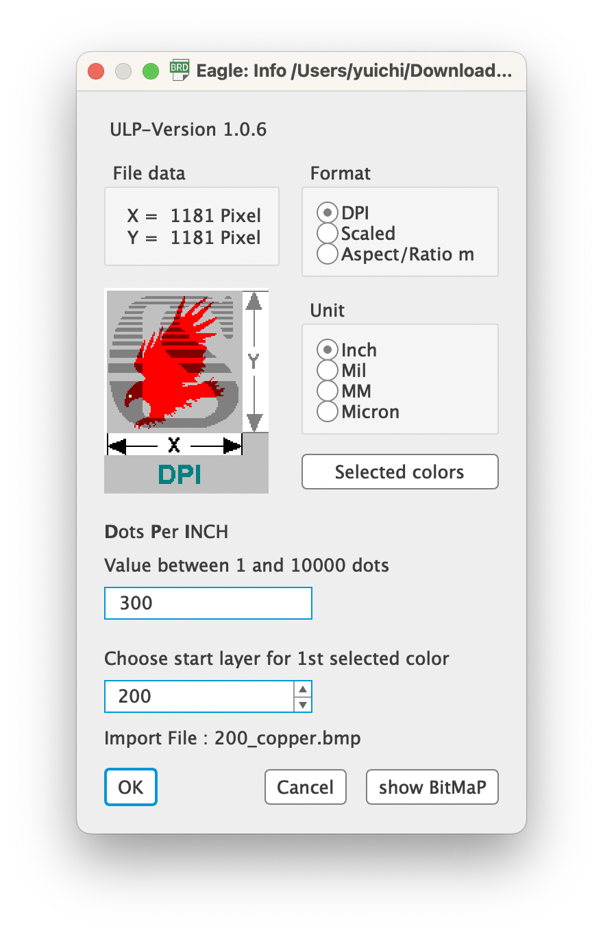
(image size: 100x100mm, 300dpi)
| JP | EN | Meaning |
|---|---|---|
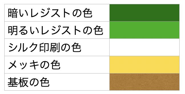 |
(1)Dark Resist (2)Light Resist (3)Silkscreen (4)Plating metal (5)FR4 PCB base |
Resist without Copper Resist on Copper Silkscreen print on any surface Plationg metal color as footplint nothing on |
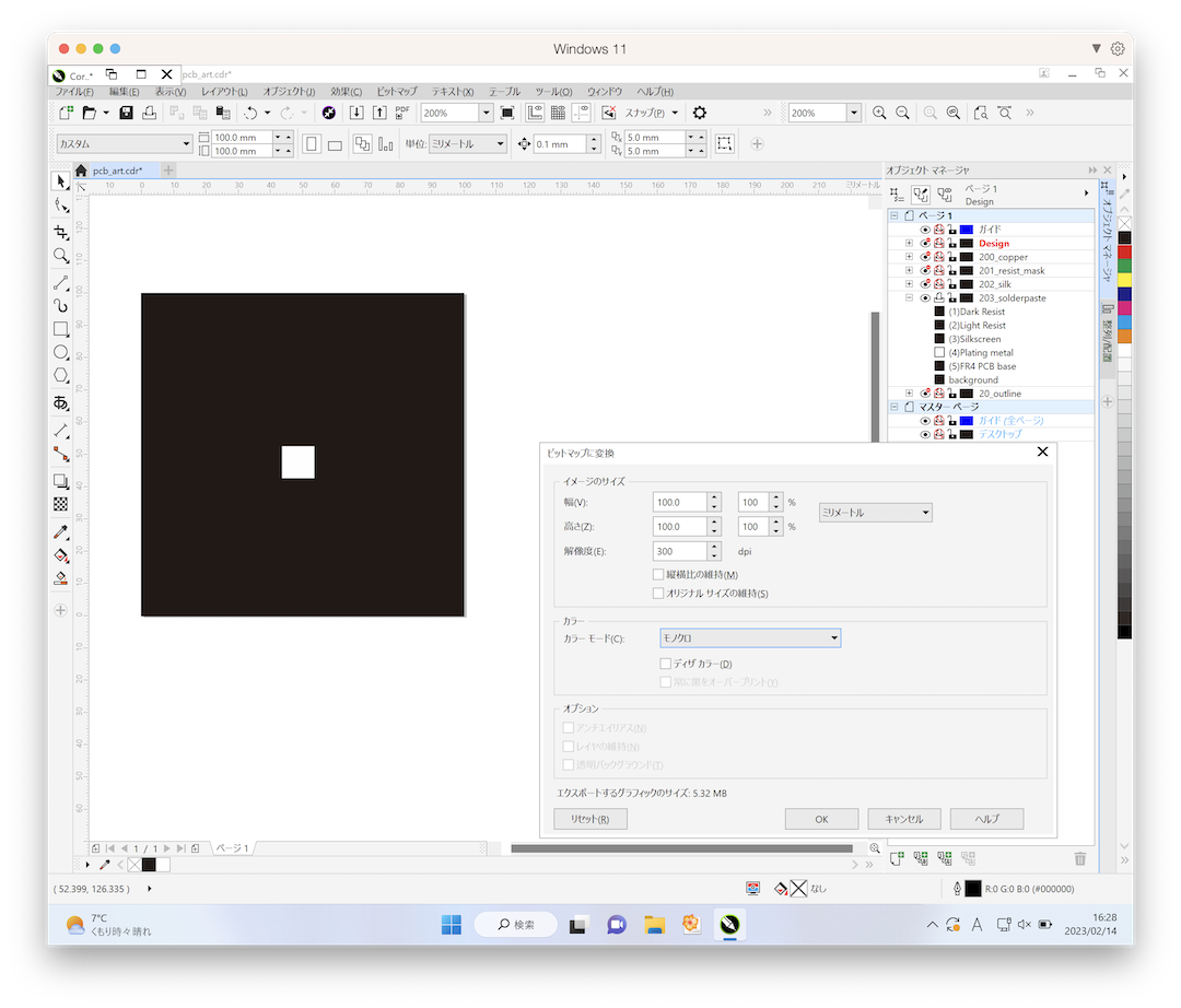
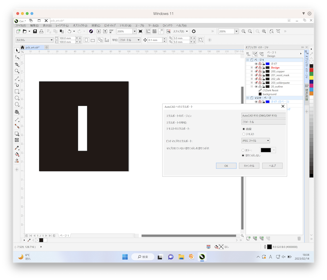
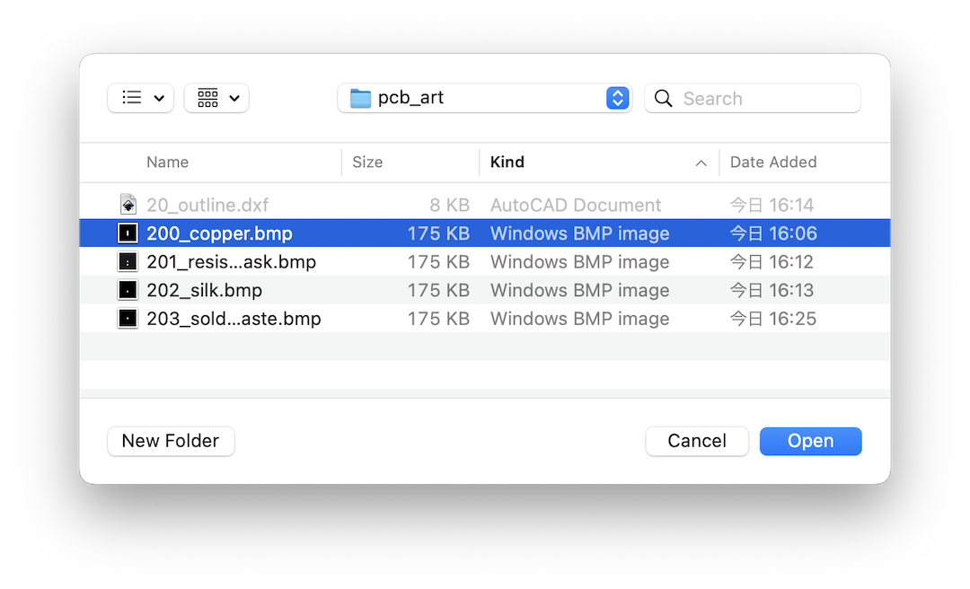
2. Make Black and white images and export to bmp and dxf
- Make layers in 2D App with these name
- Copy all color design in each layer
- Make Black and White image with Black background
- Export layers as bmp (100x100mm, 300dpi)
- Export outline as dxf (R10 should work)
| 2D App layer name | White | Black | Export format | Eagle layer No | Gerber Output File name |
|---|---|---|---|---|---|
| 200_copper | (2)Light Resist (3)Silkscreen (4)Plating metal |
(1)(5) back ground |
bmp | 200 | Top Copper |
| 201_resist_mask | (4)Plating metal (5)FR4 PCB base |
(1)(2)(3) background |
bmp | 201 | Soldermask Top |
| 202_silk | (3)Silkscreen | (1)(2)(4)(5) background |
bmp | 202 | Silkscreen Top |
| 203_solderpaste | (4)Plating metal | (1)(2)(3)(5) background |
bmp | 203 | Solderpaste Top |
| 20_outline | (1)(2)(3)(4)(5) “Weld” into one object |
background | dxf | 20 Dimention (automatically) |

Color mode: Monochrome / Black and White


Make all objects together by using “Weld” function.
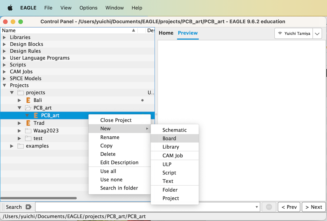
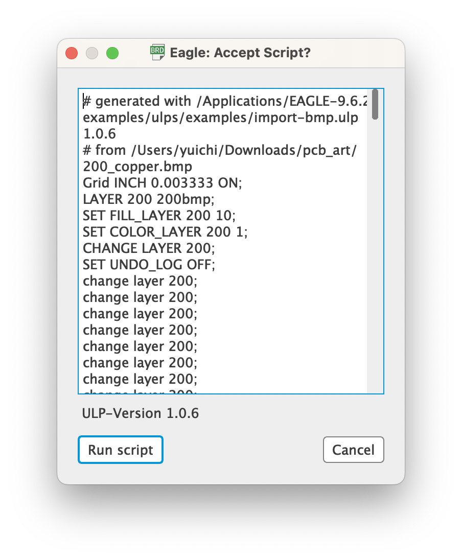
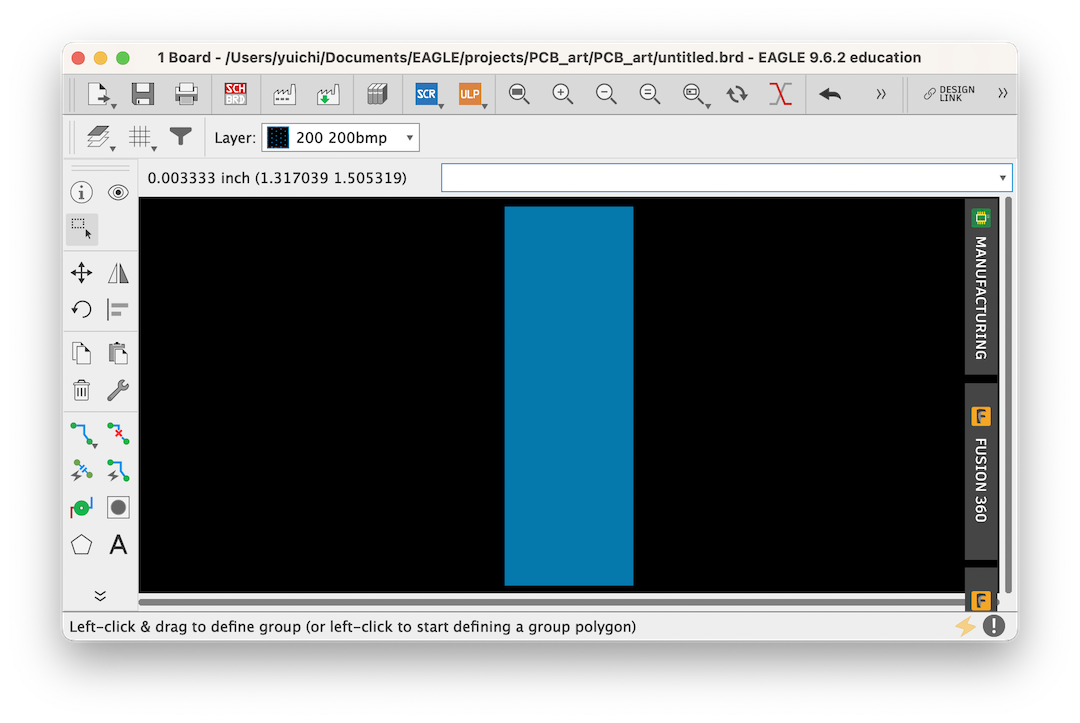
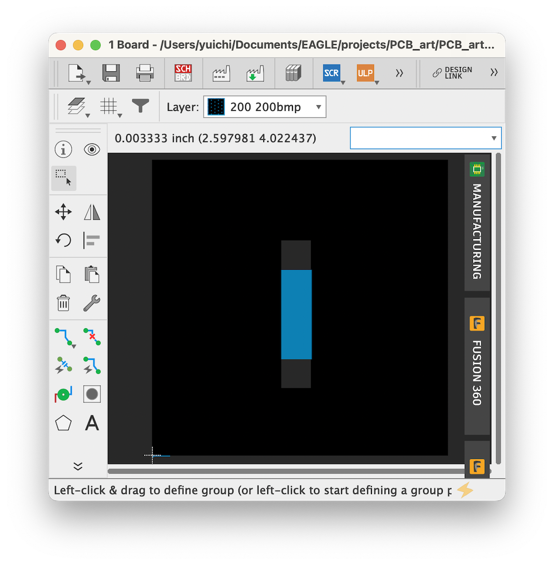
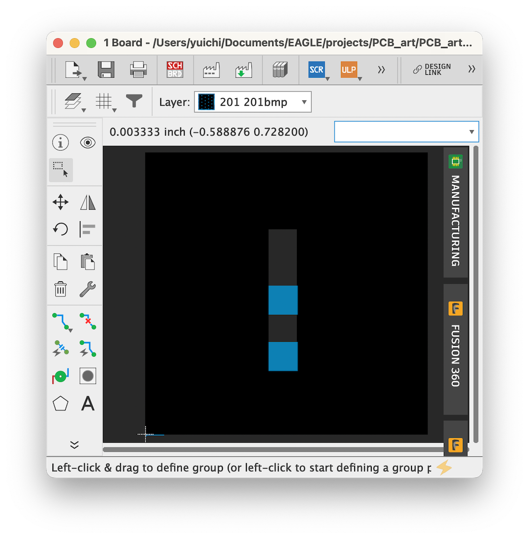
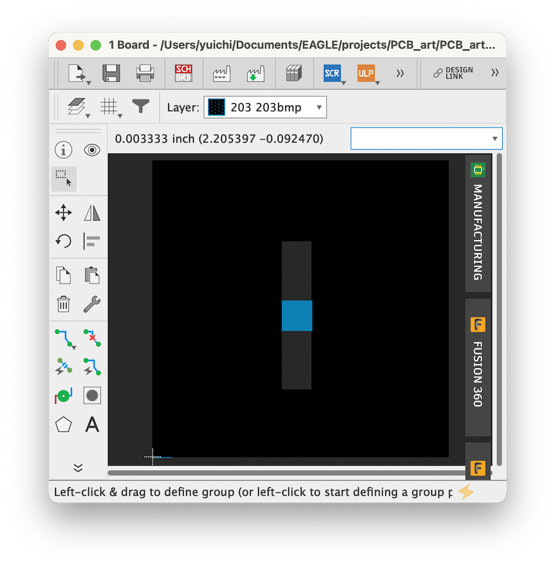
3. Import bmp and dxf in Eagle brd
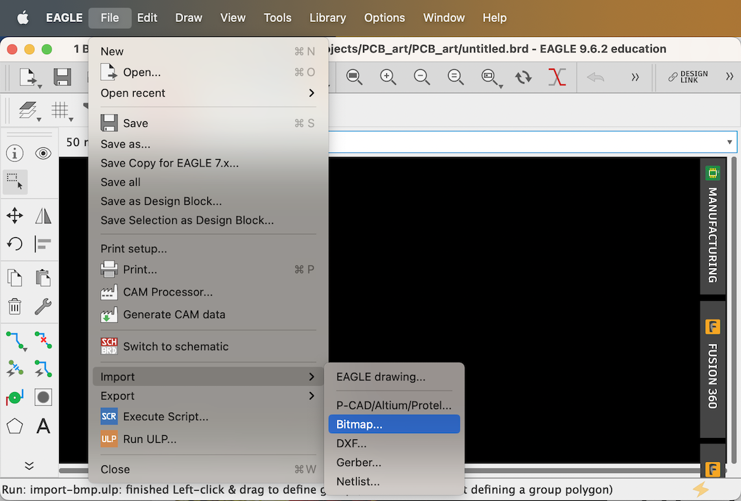
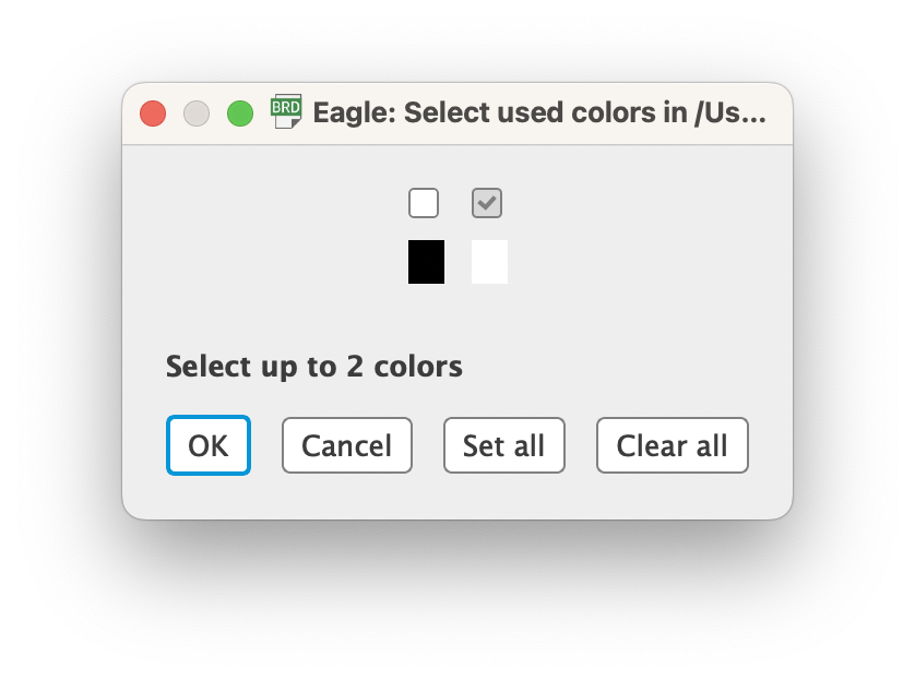
Choose start layer for 1st selected
- 200 for 200_copper.bmp
- 201 for 201_resist_mask.bmp
- 202 for 202_silk.bmp
- 203 for 203_solderpaste.bmp
| bmp/dxf | Eagle Layers |
|---|---|
200_copper.bmp |
 |
201_resist_mask.bmp |
 |
202_silk.bmp |
 |
203_solderpaste.bmp |
 |
20_outline.dxf |
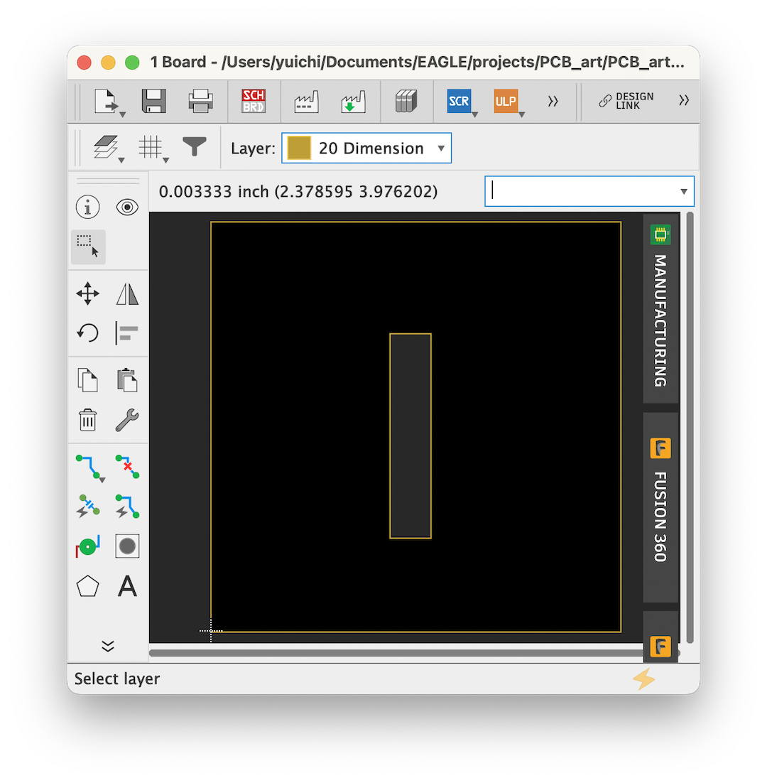 |
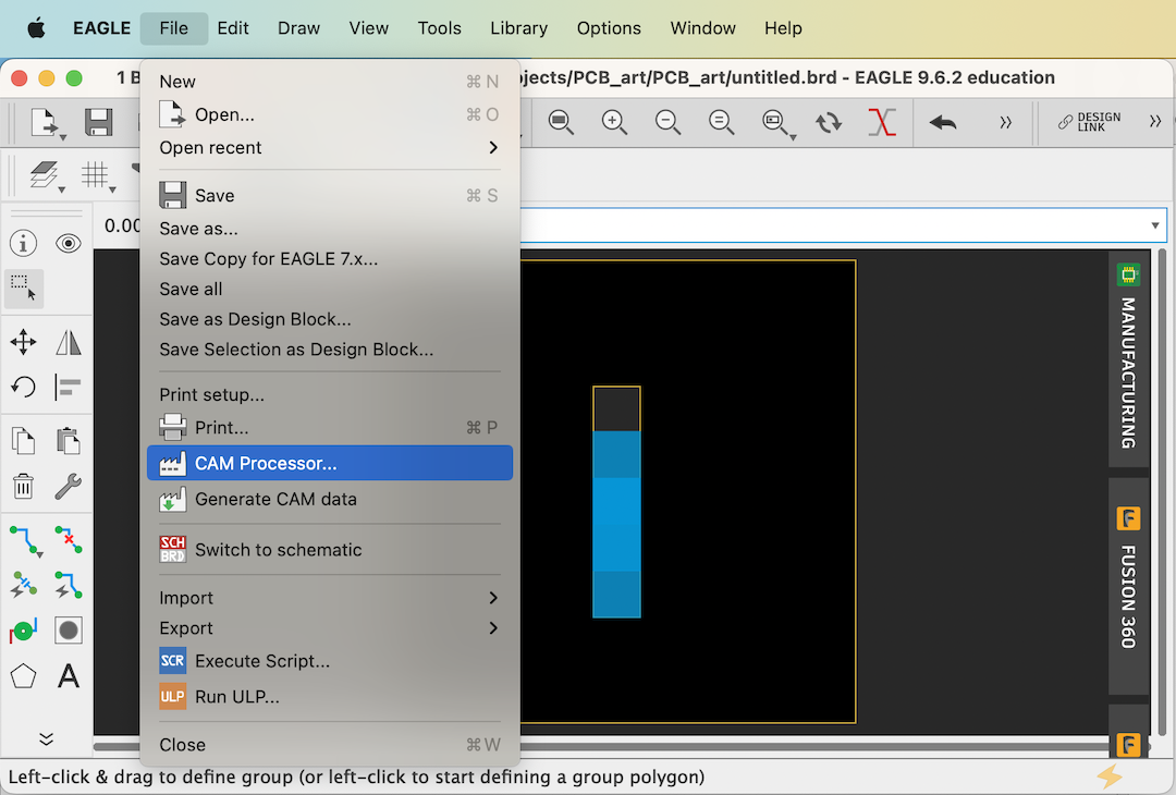
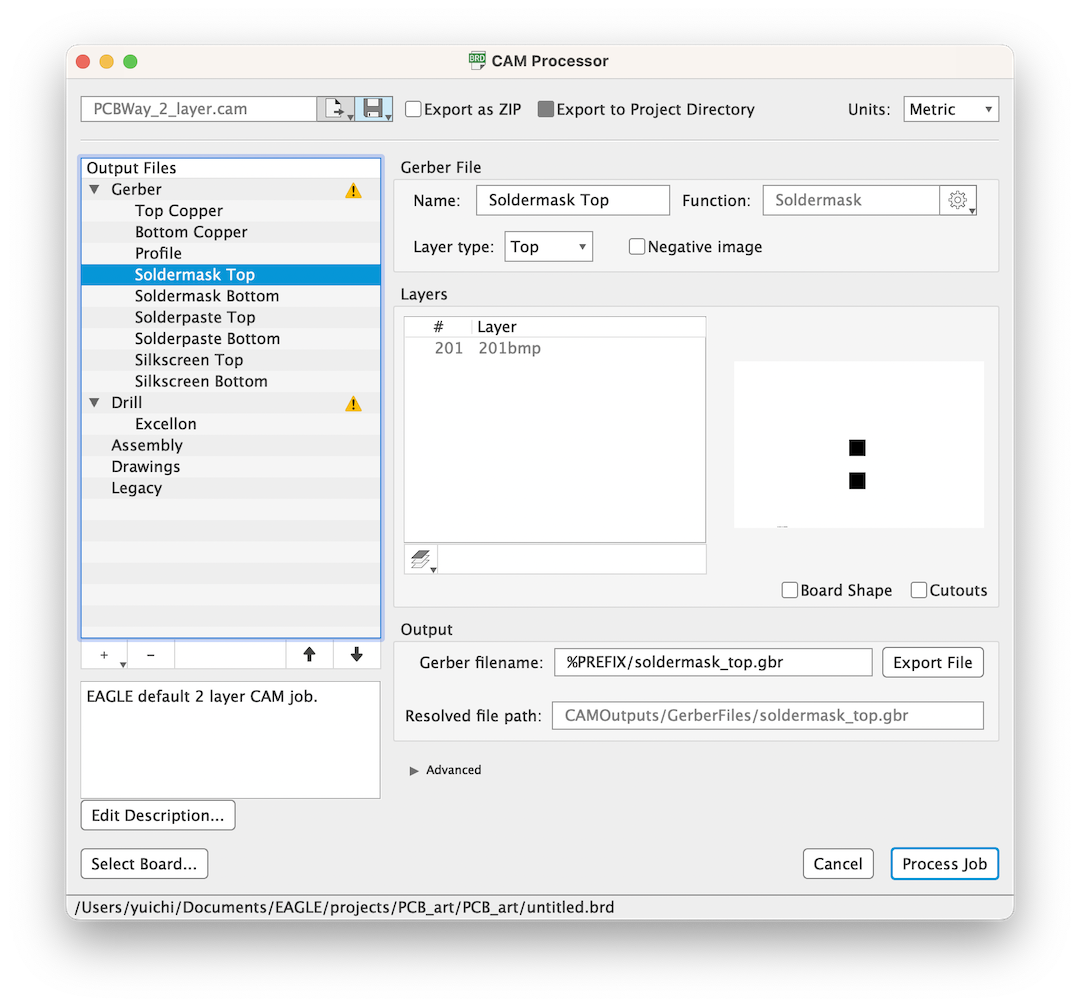
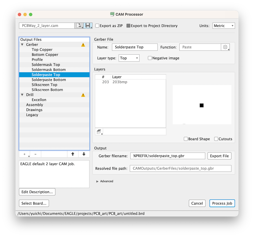
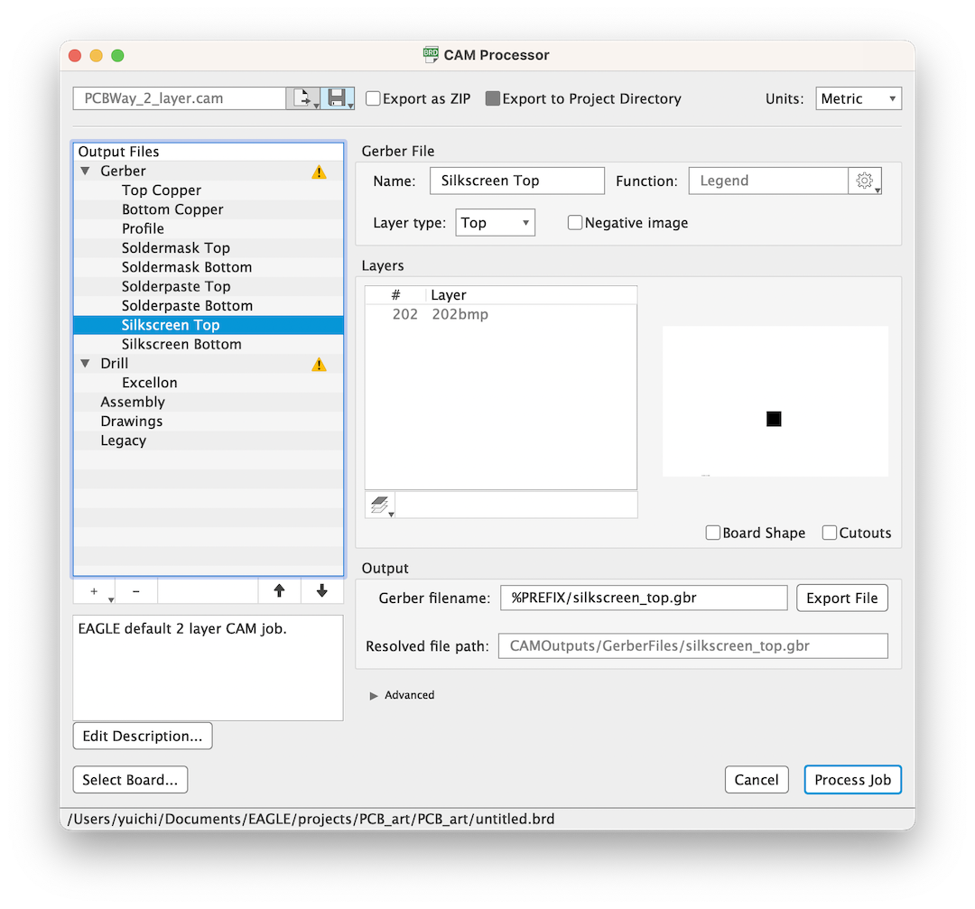
4. Set layers in Output file in CAM processor in Eagle
Go to CAM Processors
CAM job File
-
Fusion PCB
-
PCB way
-
JLC PCB
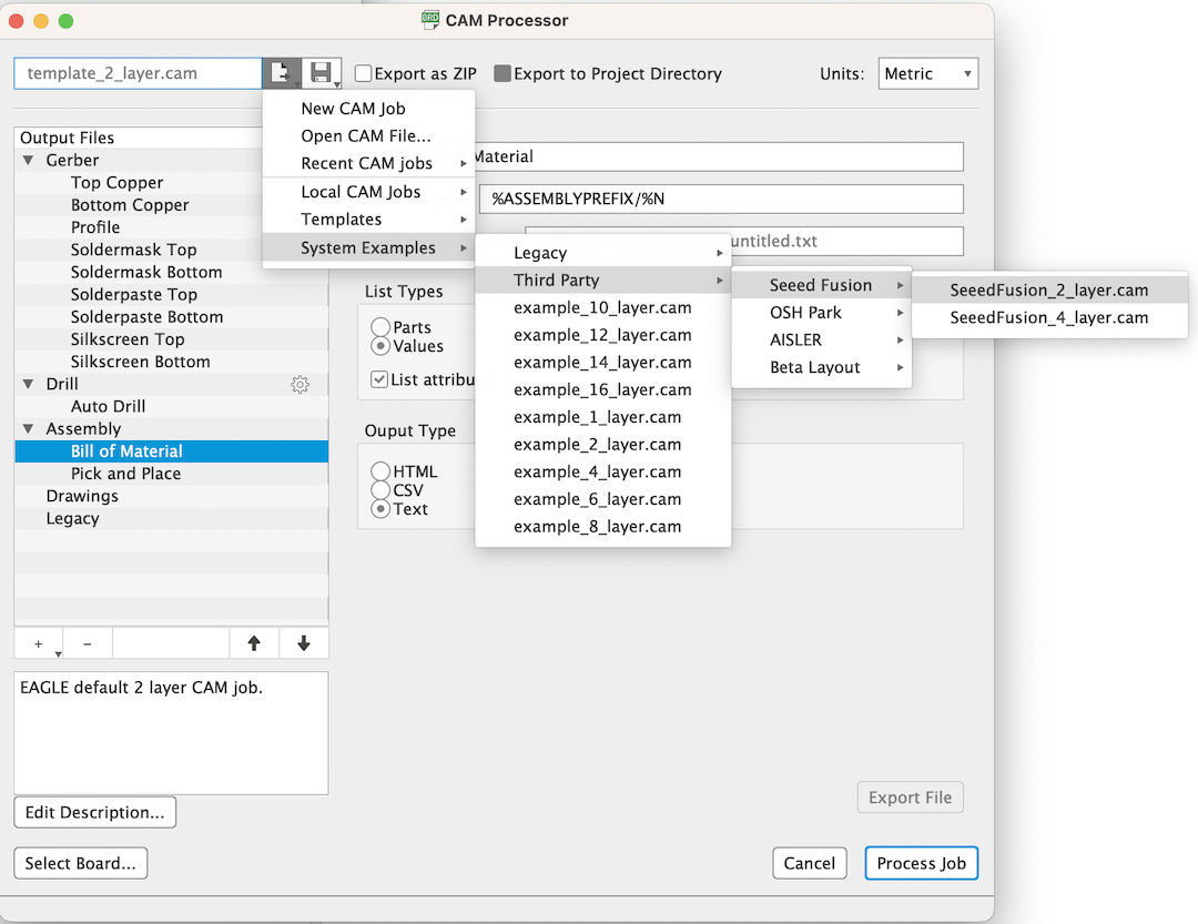
Output Files for Gerber


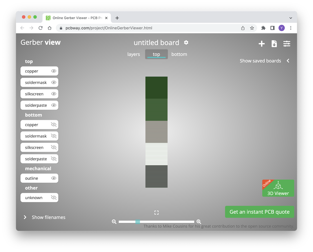
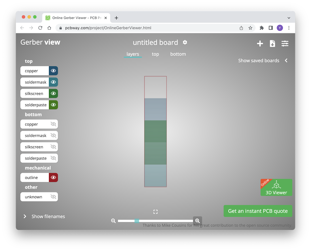
5. Gerber Viewer

Last update:
February 17, 2023